Make AI make sense
where data is created.
Femtosense builds sparse neural processors and a full AI toolchain, enabling 10× larger models and 100× better energy efficiency in tiny power-limited devices like hearing aids, TWS, appliances and defense systems.


Executive Overview
Femtosense is building the world’s most efficient sparse neural processors (SPU:
Sparse Processing Unit). Our silicon and software platform enables truly
on-device intelligence in form-factor and power-limited hardware where
traditional AI accelerators cannot operate.
With 100× energy efficiency, 10× model capacity and
$280M revenue pipeline, we are positioned to become the default AI
compute layer for hearing aids, wearables, consumer appliances, and defense
systems.
Market Opportunity
Edge AI silicon is one of the fastest-growing markets in semiconductors.
By 2026 the total addressable market reaches $15.4B+ with a CAGR of
20.6%. This surge is driven by massive demand for on-device inference in:
• Hearables & hearing aids
• TWS earbuds
• Consumer appliances (Samsung, LG, Dyson, Midea, Xiaomi, etc.)
• Industrial & robotics
• Drones and defense applications
Unlike traditional cloud AI, these environments require ultra-low power,
always-on inference and tiny silicon area—requirements that GPUs,
TPUs, and digital MAC-heavy NPUs fail to meet.
The Problem with Today’s AI Chips
Most neural network accelerators are designed for datacenter throughput, not real-world embedded constraints. They rely on dense matrix multiplications (GEMM), which wastes substantial compute on zero values, burning energy where no real work is done.
Legacy AI Accelerators
• Inefficient dense compute paths
• High energy consumption
• Require large DRAM bandwidth
• Too hot / too large for wearables
• Struggle with always-on applications
Result
Companies cannot deploy real AI into devices like hearing aids, TWS, small appliances, robotics sensors, or low-SWaP defense hardware.
The Femtosense Platform
Femtosense delivers a full-stack sparse compute solution:
1. Silicon (SPU)
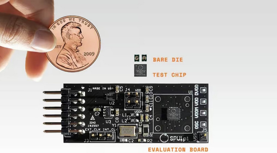
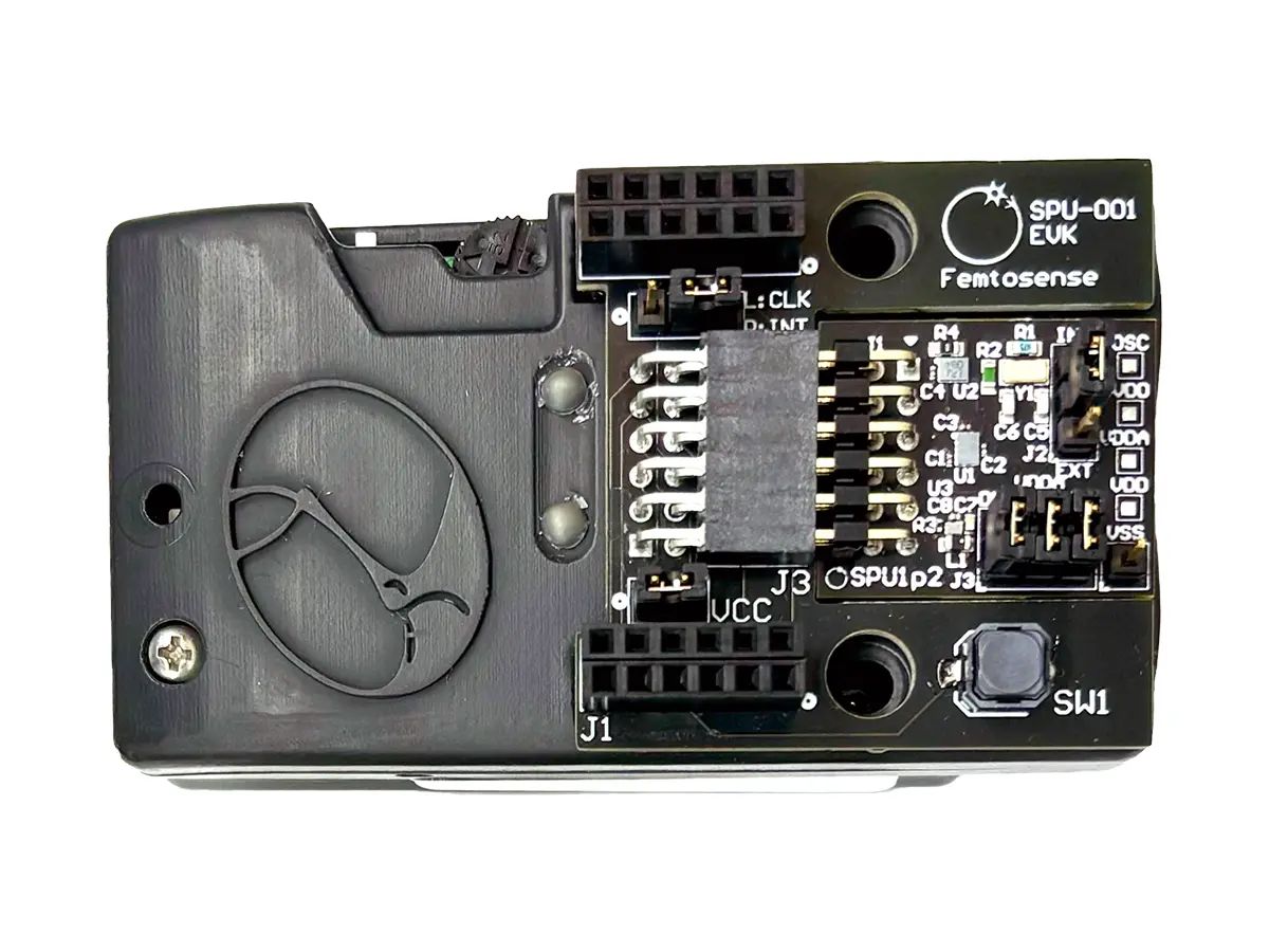
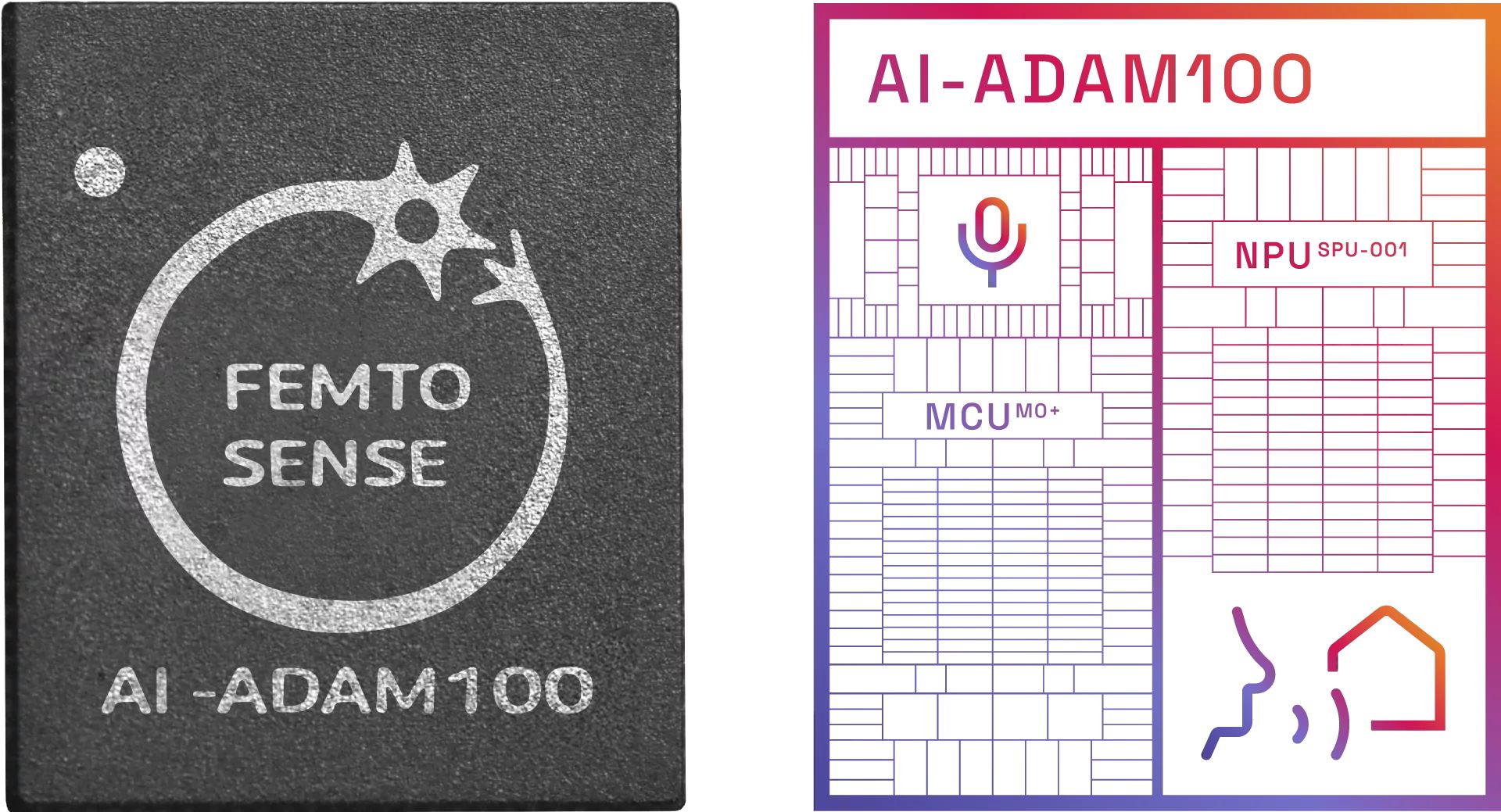
Ultra-efficient sparse neural processors enabling 100× energy efficiency with 10× model size in a tiny power envelope.
2. SDK & Toolchain
Full model conversion stack. Supports PyTorch, ONNX, TFLite with automated sparsification, quantization, pruning and deployment.
3. Applications
Reference AI models for: noise suppression, beamforming, voice control, keyword spotting, translation, audio analytics and more.
Sparse Neural Computing Technology
Modern neural networks contain 50–99% zeros after pruning,
quantization, or natural sparsity.
Yet traditional accelerators still compute on these zeros, wasting energy and
memory bandwidth.
Femtosense’s SPU (Sparse Processing Unit) eliminates this waste by computing
only the non-zero values.
This produces:
• 100× energy efficiency
• 10× effective model size
• 10× reduction in bandwidth
• Order-of-magnitude smaller silicon area
Our breakthrough sparse-math architecture is production-ready and validated
across multiple customer design wins.
Traditional Dense Compute
Dense GEMM (General Matrix Multiplication) repeatedly computes:
for i,j: sum += A[i][k] * B[k][j]
Even when A or B contains mostly zeros.
→ Massive wasted MAC operations
→ High power and large die area
Sparse Compute (Femtosense SPU)
SPU skips all zero-value computation:
for (i,k) where A[i][k] != 0: compute only on nonzeros
• Only valid operations computed
• Power scales with actual information density
• Delivers extreme energy efficiency
SPU Silicon Performance
Femtosense’s SPU family features a novel sparse-math pipeline enabling industry-leading edge inference performance.
Energy Efficiency
Industry-leading sparse compute efficiency
Model Capacity
Run models 10× larger under same power budget
Power Consumption
Always-on intelligence with minimal drain
Silicon Features
- Highly parallel sparse array compute
- Configurable inference pipelines
- Quantization-aware execution (4–8 bit)
- On-chip memory optimized for sparse ops
- Low-latency audio and sensor processing
- Small form factor suitable for wearables
Real-World Use Cases
Femtosense enables AI to operate where it never could before — inside ultra-small, ultra-low-power devices. From hearing aids to drones, our SPU architecture unlocks practical intelligence without the battery penalties of classical AI accelerators.

Hearing Aids
Femtosense provides 24-hour battery life versus 2 hours for legacy solutions doing dense audio AI. Noise suppression, beamforming, de-reverberation, voice enhancement — all run locally, always on, without thermal limits.

TWS Earbuds
Real-time voice enhancement, ANC, spatial audio and language processing — without cloud dependency or battery drain. Enables next-gen premium audio experiences.

Smart Appliances
Femtosense SPU is used for voice interaction, predictive maintenance and audio understanding in consumer appliances. Samsung, LG, Dyson, Bosch, Midea & Xiaomi are aggressively adopting on-device AI for next-gen IoT.

Defense & Autonomous Systems
Ultra-efficient sparse compute is ideal for low-SWaP military hardware:
drones, sensors, radios, translation equipment, battlefield audio
processing and more.
Femtosense projects have been supported by:
• U.S. Air Force (USAF)
• Special Operations Command (SOCOM)
• DoD research programs
Competitive Landscape
The Edge AI silicon market is fragmented across GPU-like NPUs, analog compute,
and classic DSP-based acceleration.
None of these architectures solve the fundamental challenge:
AI models are sparse — but existing chips assume they are dense.
Femtosense is the first production-ready architecture optimized around
actual information density, not theoretical FLOPs.
Why SPU Wins
1. Built for Sparsity
Uses a sparse ISA and compute pipeline. Unlike NPUs, sparsity is not an afterthought.
2. Tiny Power Envelope
Under 1 mW for many workloads. Enables always-on AI in wearables and IoT.
3. Production-Ready Silicon
Proven in customer chips today — unlike most sparse research projects.
Performance Benchmarks
SPU demonstrates category-leading energy efficiency and total cost efficiency. These diagrams summarize its advantage:
Company Roadmap
Femtosense has advanced sparse neural compute from Stanford research prototypes to commercial-grade silicon powering real customer products. The timeline below shows our journey toward global deployment.
2018 — 2020
Founding & Deep Tech Research
• Company founded by Stanford researchers specializing in neuromorphic computing • Early FPGA sparse compute prototypes validated • Seed funding secured • Built foundational sparsity math & model conversion pipeline
2021 — 2022
First Silicon & Commercial Validation
• SPU-001 silicon taped out successfully • Achieved 276 TOPS/W sparse efficiency • Engaged 50+ prospective customers • Collaborations with Samsung appliance ecosystem • DoD-funded projects initiated with USAF & SOCOM
2023 — 2024
Design Wins & Deployment
• Secured 4 commercial design wins • APAC and US enterprise/defense integrations begin • Joint chip with ABOV Semiconductor for appliances • First customer product lines enter EVT/DVT • Revenue line-of-sight through 2025–2026
2025 — 2026
Mass-Scale Product Rollout
• Ramp production across hearing aids, TWS, appliances, IoT • Expansion into industrial audio analytics • Defense and UAV platform-scale adoption • Revenue scaling from multi-million to tens-of-millions • Next-gen SPU silicon line enters execution phase
Business Model
Femtosense monetizes through multiple revenue channels tied to silicon, software, and long-term customer relationships.
1. Silicon Sales
Revenue from SPU chip units shipped through our partner fabs and appliance/ device OEM integrations.
2. Licensing & Royalties
Per-unit royalties from semiconductor and IoT partners integrating SPU IP into their SOCs or chipsets.
3. Software & SDK
SDK licensing for enterprise customers, including advanced sparsification tools and model optimization pipelines.
Financial Projection (2024 – 2026)
With 4 design wins and a robust customer pipeline, Femtosense anticipates strong revenue growth as SPU-powered products enter global markets.
2024
EVT/DVT customers begin sampling
2025
Initial product shipments
2026
Multiple segments at scale
World-Class Team
Femtosense is built by experts in sparse machine learning, silicon architecture, neuroscience-inspired computation, and large-scale systems engineering.

CEO — Dr. Alex Chen
PhD, Stanford University — neuromorphic compute & AI hardware. Led silicon R&D for multiple AI accelerator tapeouts.

CTO — Dr. Maya Lee
PhD, Stanford — Sparse ML research pioneer. Created Femtosense’s sparsification algorithms & toolchain.

Head of ML — Kevin Zhou
Ex-Google Research. 8+ years building production ML systems, audio AI, and embedded inference.
Advisory Board
Prof. Elena Marks — Stanford
Pioneer in computational neuroscience and sparse representations. Advisor for algorithmic architecture and model optimization.
Dr. Javier Ortiz — Ex-Qualcomm VP
Former VP of Engineering, Snapdragon Platform. Advises on commercialization and OEM partnerships.
Investors & Supporters
Femtosense is backed by Silicon Valley VCs, strategic partners in consumer electronics, and US government innovation programs.
Silicon Valley VC Fund
Deep tech investor with portfolio in semiconductors and AI.
Strategic Appliance/OEM Partner
Global consumer electronics group supporting SPU integration.
DoD Innovation Program
Funding received via USAF & SOCOM for high-efficiency compute R&D.
Get in Touch
Whether you are building hearing aids, TWS earbuds, smart appliances, industrial
sensors or low-SWaP defense hardware, Femtosense can help you bring real AI
intelligence directly onto your devices.
Share a few details and our team will follow up with technical resources,
evaluation kits, and roadmap discussions.
Talk to Our Team
For technical deep dives, SPU evaluation kits, joint development, and investment-related questions, contact:
Femtosense Business Development
Email: hello@femtosense.xyz
Twitter/X: @Femto_AI
HQ: San Francisco Bay Area, California